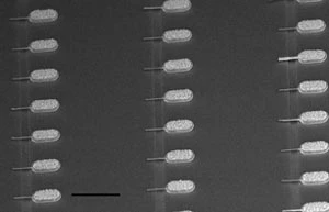
"Diagnostic chips can be made more useful by assembling, at predetermined locations on the chip, large numbers of nanowires pretreated off chip," says Rustom B. Bhiladvala, research assistant professor, electrical engineering. "Using this new bottom-up method, our group has demonstrated that thousands of single wires can be successfully aligned and anchored to form tiny diving board resonator arrays."
The traditional top-down process begins with silicon and carves nanoresonator devices from the material. This approach works well, producing many devices that are nearly identical, but the process has limitations. The addition of chemical probes or other changes in the existing materials must be done after the devices are fabricated on the chips.
The bottom-up method, although not producing identical devices, is more flexible. In bottom-up fabrication, researchers manufacture nanowires off chip using any inorganic or organic material that will produce nanowires. They can attach probe molecules to the wires off chip, using a variety of chemicals and they can attach each group of nanowires and their probes to the chips in the numbers and at the locations desired.
"We can achieve high device integration yields, but the devices are not as uniform as top-down manufactured devices," says Theresa S. Mayer, professor of electrical engineering. "However, we can access materials that are not easy to integrate into the devices with top-down methods. We can also integrate wires treated off-chip with entirely different probe molecules that are attached to the wires using condition optimized for that molecule."
The researchers fabricated these proof-of-concept chips with nanowires made of single crystal silicon or polycrystalline rhodium attached at one end and suspended over a depression. This type of device can detect target molecules when they bind to the probe molecules on the nanowires, changing the wire's vibration.
To create the bottom-up diving board resonators, the researchers used a layer of photoresist – a light-sensitive material which, when exposed to light, can then be easily removed chemically – to create an array of tiny rectangular wells on the chip. These wells were aligned above an insulated electrode on the chip surface. A solution of nanowires, with probes already attached, flows over the chip surface while the electrodes produce an electric field. The electric field grabs the nanowires and pulls them to the surface where they align perpendicularly to the electrode. The aligned nanowires skate along the electrodes and when they reach a well, drop down into it.
Once a wire is in a well, that wire repels other wires allowing, for the most part, only one wire per well. The number of wires in the solution is controlled depending on the number of wells, so only a few wires remain on the chip outside the wells.
In the case of the resonators, once the wires are in the depressions, the RhNW resonator arrays showing a high yield of single NWs positioned at predefined locations on the chip. researchers switch to a top-down approach, placing a layer of a different photoresist on top of the chip and removing a small cube of photoresist around the tip, where the wire anchor will be built. The researchers then electro-deposit metal into the tiny square holes, anchoring the nanowire in place. They dissolve the photoresist, leaving the suspended nanowire and at the same time removing the nanowires that did not make it into wells.
By choosing the well depth and the thickness of the original photoresist layer, the researchers can adjust the height of the resonator above the chip surface. An added benefit of bottom-up fabrication is that the nanowires with their probe molecules retain their functionality after integration. The researchers also showed that, after the resonator chip arrays were fabricated, target molecules did selectively bind to only those nanowires treated with the correct probe molecules.
"Bottom-up fabrication is an entirely new nanomanufacturing approach and we need to create devices that have properties that match what we can now make using topdown fabrication," Mayer says. "Our vision is to make large arrays of nano size devices with multiple probes for multiple targets by placing different groups of functionalized nanowires sequentially on chips."

Explore the May 2008 Issue
Check out more from this issue and find your next story to read.
Latest from Today's Medical Developments
- HERMES AWARD 2025 – Jury nominates three tech innovations
- Vision Engineering’s EVO Cam HALO
- How to Reduce First Article Inspection Creation Time by 70% to 90% with DISCUS Software
- FANUC America launches new robot tutorial website for all
- Murata Machinery USA’s MT1065EX twin-spindle, CNC turning center
- #40 - Lunch & Learn with Fagor Automation
- Kistler offers service for piezoelectric force sensors and measuring chains
- Creaform’s Pro version of Scan-to-CAD Application Module


