Nanofabrica
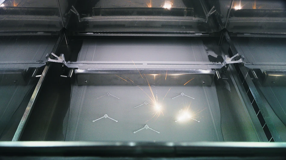
Nanofabrica has developed a micron-level resolution additive manufacturing (AM) platform, providing an end-to-end custom solution to manufacturers requiring micron and sub-micron levels of resolution and surface finish.
To date, key AM platform developers struggle to get resolution under 50 microns, and the few companies that have strived to provide a micro-manufacturing AM solution are either extremely expensive, extremely slow, or can only print parts very restricted in size.
Nanofabrica has identified a series of applications in the area of optics, semi-conductors, micro-electronics, MEMS, micro-fluidics, and life sciences, ideal for AM micro-manufacturing. Products such as casing for micro-electronics, micro-springs, micro-actuators, and micro-sensors, and numerous medical applications such as micro-valves, micro-syringes, and micro-implantable or surgical devices.
How the process works
The first breakthrough of Nanofabrica’s technology enables high precision at a cost required for industrial manufacturing. Nanofabrica’s AM process is based on a technology that is well known in the AM world – a Digital Light Processor (DLP) engine – but to achieve repeatable micron levels of resolution combines DLP with the use of adaptive optics. This tool, in conjunction with an array of sensors, allows for a closed feedback loop; the core element enabling Nanofabrica’s product to reach very high accuracy while remaining cost-effective as a manufacturing solution. Where all other AM platform developers in this space achieve precision through great hardware, Nanofabrica tackles this issue with software where solutions are easier, more robust, and less expensive. Adaptive optics have been used in other areas of technology, but this is the first time that they have been applied to an AM technology.

Another aspect of Nanofabrica’s AM platform is the ability to achieve micron resolution over centimeter-sized parts. To enable this, a number of technologies have been combined.
Specifically, the company has taken its innovative use of adaptive optics and enhanced this imaging unit with technology and know-how used in the semiconductor industry. By working at the intersection of semiconductors and AM, Nanofabrica can build large macro parts with intricate micro details. It can also do this at speed by introducing a multi-resolution strategy; parts where fine details are required are printed relatively slowly, but in the areas where the details aren’t so exacting, the part is printed at a speeds 10x to 100x faster, making the entire printing speed 5x to 100x faster than other micro AM platforms.
In addition, for OEMs requiring small parts, thousands of parts can be printed in a single build on the Nanofabrica platform, making it a true mass manufacturing technology for micro-product or component manufacturers.
The multi-resolution capability is possible through hardware that enables a tradeoff between speed and resolution, and software algorithms which prepare the part and printing path by defining and sectioning it into low- and high-resolution areas, which are fed into the printer path and machine parameters. There are not only two resolutions but a spectrum of resolutions that allow speed to be optimized while maintaining satisfactory results throughout the part.
The final algorithm family focuses on file preparation, optimizing parameters such as print angle build plate, supports, etc., which ensure a precise, optimized, and reliable print process.
Nanofabrica has also developed its own proprietary materials (based on the most commonly used industry polymers) which enable ultra-high resolution in parts built.

What does this mean for manufacturers?
The Nanofabrica AM technology brings AM into new markets and enables new applications, especially for manufacturers requiring micron and sub-micron level accuracy and resolution. Since AM is relatively agnostic to part complexity, it is possible to design and manufacture unique geometries and the Nanofabrica technology has become an enabling technology.
AM also requires no set up costs. The tooling required for traditional manufacturing processes not only has a negative impact on time to market, but also makes such processes uneconomic for small or medium sized production runs. For AM technologies, small and medium sized runs are cost-effective, and today, represents the sweet spot for the technology.
Add into the mix that AM allows for mass customization, personalization, and the ability to use the same manufacturing platform for prototyping, small batches, and mass manufacturing, and you begin to see the myriad of possibilities that now exist for micro manufacturers.

Customized solutions
As designer engineers and manufacturers assess the possibilities that exist for the use of AM to replace or, more likely, sit alongside traditional manufacturing processes, there needs to be a quantum shift in the way that they approach the entire design to manufacturing process.
This begins with re-evaluating product design, and the subject of design for additive manufacturing (DfAM) has become a fertile area for discussion and debate today.
While AM users are beginning to take advantage of DfAM for macro AM platforms, there is little to no understanding of the DfAM issues when using AM for micro applications. Addressing this, Nanofabrica promotes a collaborative relationship with its customers to locate the opportunities and avoid traps that exist when adopting – or considering adopting – AM for production purposes in the micro-manufacturing arena.
Existing at the interface of AM for production and the industry-wide drive towards miniaturization, Nanofabrica’s micro AM technology lifts the lid for designers and manufacturers in their quest to embrace the inherent advantage of AM, and at last to be able to exploit the ability that exists with AM to build complex parts in small, medium, and high volumes in a timely and cost-effective fashion.
Latest from Today's Medical Developments
- How to Reduce First Article Inspection Creation Time by 70% to 90% with DISCUS Software
- FANUC America launches new robot tutorial website for all
- Murata Machinery USA’s MT1065EX twin-spindle, CNC turning center
- #40 - Lunch & Learn with Fagor Automation
- Kistler offers service for piezoelectric force sensors and measuring chains
- Creaform’s Pro version of Scan-to-CAD Application Module
- Humanoid robots to become the next US-China battleground
- Air Turbine Technology’s Air Turbine Spindles 601 Series


